Keywords: Graphene Symmetry Breaking Antiferromagnetic Insulation Polarized Insulator
Note: This article uses the Sine Scientific Instruments OE1201 lock-in amplifier to make measurement.
[Overview]
In September 2023, Associate Professor Guorui Chen's team at the Key Laboratory of Artificial Structures and Quantum Regulation of the Ministry of Education, Shanghai Jiao Tong University, collaborated with Jeil Jung's team at Seoul National University, Korea, to publish an article in Nature titled "Spontaneous broken-symmetry insulator and metals in tetralayer rhombohedral graphene". The article demonstrates that crystalline multilayer graphene is an ideal platform for studying various symmetry breaking driven by Coulomb interactions.
Graphene's charge carriers can cause multiple simplicity to break spontaneously. Coulomb interactions become dominant as the number of graphene layers in a rhombic stack increases, due to significant kinetic energy. This study used phonon-polariton assisted near-field infrared imaging to determine the stacking order of four-layer graphene devices. The study observed a series of spontaneous symmetry breaking and its leaps through quantum transport measurements. The carrier density n and potential shift field D were finely tuned for accuracy. At n=D=0, the study results in a layered antiferromagnetic insulator with an energy gap of approximately 15 meV. Increasing D allows for a continuous phase transition from a layered antiferromagnetic insulator to a layered polarized insulator. Simultaneously tuning n and D results in isotropic spin-polarized metals, including spin-valley polarized and spin-polarized metals. These transitions are associated with changes in the Fermi surface's topology and are consistent with the Stoner criterion.

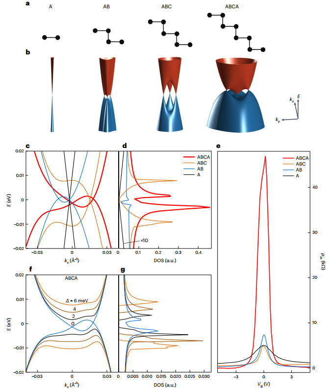
Fig. 1 Family of rhombic graphenes
In cases where Coulomb interaction dominates, the spins and energy valleys in graphene may no longer be simple, and the competition between energy bands with different degrees of freedom can result in numerous symmetry breakings. However, for monolayer graphene (as shown in Fig. 1a), the linear energy band dispersion prevents spontaneous symmetry breaking due to the larger kinetic energy.
Figures 1a and b display the cell and energy band structure calculated at the K-point from single-layer rhombic graphene to ABCA four-layer rhombic graphene (ABCA-ALG). The interlayer jumps cause a significant triangular warping and an increased VanHove singularity (VHS) near the electrically neutral point (CNP), as shown in the energy band diagrams and density of states maps (Fig. 1c, d).
The strong Coulomb interaction can cause the destabilization of the Fermi circle due to the high density of states at CNP and VHS. This can result in the creation of new ground states with symmetry breaking. The energy band structure and correlation of rhombic graphene ground can be modulated by the vertical potential shift field D, which contributes to the energy difference Δ between the top and bottom of the band (see Fig. 1f, g). ABCA-4LG can open an energy gap at the CNP while changing its correlation, layer polarization, and VHS. Specifically, this means that ABCA-4LG has the ability to alter the properties of the CNP in multiple ways.
It is important to note that all graphene layers in Fig. 1e are on a hexagonal boron nitride (hBN) substrate, mitigating qualitative differences in electron-hole pair pits, charge mobility, and dielectric shielding effects. Therefore, the large resistivity peaks observed in ABCA-4LG are considered to be intrinsic.
[Samples & Tests]

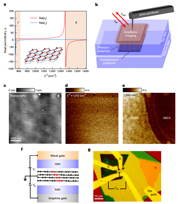
Fig. 2 Photon-polariton assisted near-field optical imaging of stacked graphene under hBN coverage
Bulk graphene and exfoliated thin layers naturally have rhombic stacking, but it is energetically unstable and can easily convert to Bernal stacking during preparation (e.g., dry transfer). Therefore, it is crucial to monitor the stacking order effectively throughout the preparation process, especially after hBN coverage. Traditional tools like Raman spectroscopy are not applicable in these cases.
To tackle this challenge, the study uses a phonon-polariton assisted near-field optical imaging technique. This technique enables the identification of rhombic and Bernal graphene under hBN coverage. The imaging was performed on a scanning near-field optical microscope (SNOM) system.
When hBN covers graphene, conventional near-field optical imaging of graphene becomes impossible due to the highly localized near-field and the strong shielding effect of hBN sheets. The study carefully selected a specific excitation frequency located in one of the Reststrahlen bands of the hBN (Fig. 2a) to image the graphene embedded in the middle. At this frequency, the hBN acts as a waveguide, transmitting the optical response of the graphene located below it to its top surface (Fig. 2b).
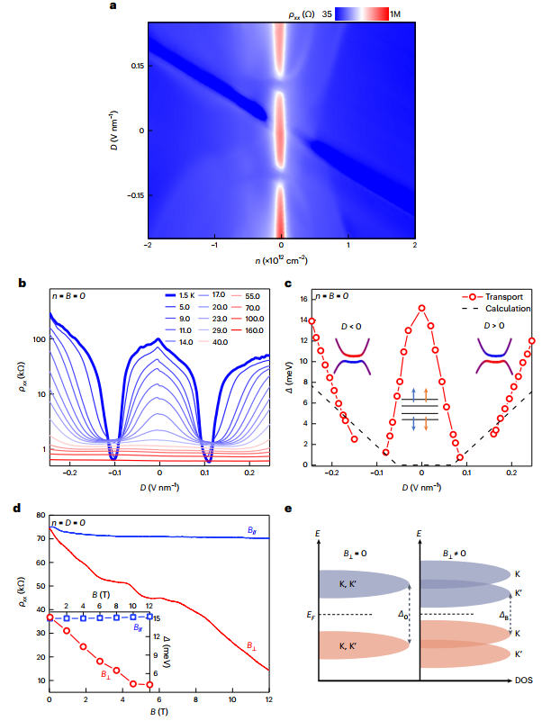
Fig. 3 Symmetry breaking at n = 0
Quantum transport measurements were accomplished in an Oxford plug-in variable-temperature system at a base temperature of 1.5 K. The measurement was performed with a Sine Scientific Instruments lock-in amplifier, OE1201, at a frequency of 17 Hz. The resistivity was measured by means of a Sine Scientific Instruments lock-in amplifier OE1201 (generating an AC current with an amplitude of 10 nA and a frequency of 17 Hz) used in conjunction with a 100 MΩ resistor, with a gate voltage applied using a source meter Keithley 2400. The displacement field D is set by D=(Db+Dt)/2 and the carrier density is determined by n=(Db-Dt)/2. Here, Db=+εb(Vb-Vb0)db and Dt=-εt(Vt-Vt0)dt. where ε and d are the dielectric constant and the thickness of the dielectric layer, respectively; and Vb0 and Vt0 are the effective offset voltages induced by environmentally-induced carrier doping.
Two distinct insulating phases, D = 0 and D ≠ 0, were observed at the charge neutral point (n = 0) by quantum transport measurements (Fig. a), and the color map represents the variation of conductivity with n and D at T = 1.5 K. The color map shows the relationship between the conductivity and D at T = 1.5 K. Figure b further confirms the insulating properties of these two phases by means of temperature-resistivity curves. In addition, it can be observed that the transport energy gap of the insulator at n = D = 0 decreases linearly with D and finally disappears at |D| ≈ 0.1 (Fig. c). For insulators with D ≠ 0, the energy gap appears and increases linearly with |D| when |D| > 0.15. The two insulating phases are connected by a low-resistance region, which is located at |D| ≈ 0.10-0.15 .

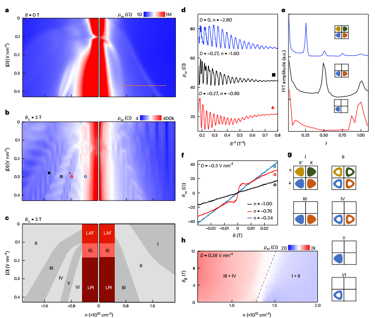
Fig. 4 Symmetry-breaking metal in ABCA-4LG
Figure 4a emphasizes the resistivity of the hole side at negative D and the electron side at positive D due to the presence of P-N junctions formed by a mismatch of opposite sign between the top and bottom gates. The metal regions with different behaviors are separated by resistivity peaks, as shown by the white lines in the figure. In a perpendicular magnetic field of B = 3 T, Landau energy levels with varying degrees of complexity are formed (Fig. 4b).
To investigate the degree of simplicity in different regions, the study kept n and D constant in the three regions and directly measured the variation of quantum oscillations with the perpendicular magnetic field B. Figure 4d shows the quantum oscillations in the three regions. Figure 4e displays the fast Fourier transform of the quantum oscillations in Figure. 4d, revealing the dominant peaks in each region located at f = 1/4, 1/2, and 1. These frequencies correspond to quadruple-simplex, dual-simplex, and single-simplex energy bands, respectively.


