Lock-in amplifier
Lock-in amplifiers are used to detect and measure very small AC signals. Accurate measurements may be made even when the small signal is obscured by noise sources many thousands of times larger.
Lock-in amplifier is a small signals detection means based on the coherence method. Lock-in amplifiers use a key technique named as phase-sensitive detection (PSD) to single out the required component of one signal. The component has the same frequency and the fixed phase differences with the reference signal. Noise signals at frequencies other than the reference frequency are rejected and do not affect the measurement.
Let's consider an example. Suppose the signal is a 10 nV sine wave at 10 kHz. A good low noise amplifier will have about 5 nV/√Hz of input noise.
① If the amplifier bandwidth is 100 kHz and the gain is 1000, then we can expect our output to be 10 µV of signal (10 nV x 1000) and 1.6 mV of broadband noise (5 nV/√Hz x √100 kHz x 1000). We won't have much luck measuring the output signal unless we
single out the frequency of interest.
② If we follow the amplifier with a band pass filter with a Q=100 (a VERY good filter) centered at 10 kHz, any signal in a 100 Hz bandwidth will be detected (10 kHz/Q). The noise in the filter pass band will be 50 µV (5 nV/√Hz x √100 Hz x 1000) and the signal will still be 10 µV. The output noise is much greater than the signal and an accurate measurement can not be made. Further gain will not help the signal to noise problem.
③ Now try following the amplifier with a phasesensitive detector (PSD). The PSD can detect the signal at 10 kHz with a bandwidth as narrow as 0.01 Hz! In this case, the noise in the detection bandwidth will be only 0.5 µV (5 nV/√Hz x √.01 Hz x 1000) while the signal is still 10 µV. The signal to noise ratio is now 20 and an accurate measurement of the signal is possible.
Phase-sensitive detection
As we said before, PSD can be seen as a very narrow bandwidth band-pass filter. The basic PSD modules include one multiplier module and one low-pass filter (LPF) module, as Fig.1 shows. Sometimes PSD is known as the multiplier module without LPF.

Fig.1 Phase sensitive detection diagram
In Fig.1, S_I (t) is the input signal plus noise in time region, S_R (t) is the reference signal which has a fixed frequency and phase.

Fig.2 Single-phase amplifier diagram
In Fig.2, the input signal S_I (t) is defined as:S_I (t)=A_I sin〖(ωt+φ)+B(t)〗 , where ω is the input signal frequency, A_I sin(ωt+φ) is the input signal, B(t) is the total noise. And the reference signal S_R (t) can be defined as: S_R (t)=A_R sin(ωt+δ).
The PSD output signal is defined as:
S_psd=S_I (t) S_R (t)=A_I A_R sin【(ωt+φ) sin(ωt+δ)+B(t)A_R】sin(ωt+δ)
=1/2 A_I A_R cos【(φ-δ)】-1/2 A_I A_R cos( 2ωt+φ+δ)+B(t)A_R sin(ωt+δ)
In weak signal detection, people have different requirements for performance according to different situations.For example, in temperature detection, low frequency applications are often required because of the hysteresis of thermal effects.In the field of radio frequency weak signal detection, it is no doubt that the equipment can respond to high-speed signal.In biological detection experiments, the SNR is generally low, so the requirements of equipment are often focused on its signal extraction ability.In optical applications, it is usually necessary to detect weak current signals, which requires the equipment to have current amplification capability.In a word, there are many requirements for the PLL amplifier. For the sake of unification, the main performance parameters of the PLL amplifier are summarized and condensed.
1. Input Level FS (Full Scale Input Level) At Full Scale Output
FS is sometimes called Full Scale Sensitivity, which is used to characterize the measurement Sensitivity of the phase-locked amplifier. It has the dimension of voltage and is related to the total gain of the system, as follows:
FS=OUTmax/Atotal
2. Overload Level (OVL)
Where, OUTmax indicates the output of the full scale value, such as 10V; Atotal represents the total gain capability of the system, for example, 1e-7; So the FS of the system is 1uV.FS actually refers to the amplification capability of the system.
It should be noted that "output" refers to a representation of the useful signal measured by the phase-locked amplifier. This representation is generally the effective value of the input signal, and sometimes the output may be the effective value of the useful signal measured by controllable adjustment for the needs of application.OE series phase-locked amplifier can be directly input 1Vrms signal for measurement, its sensitivity from 1NVRMS-1VRMS according to the order of 1-2-5 calibration, so that users can easily adjust the signal of different sizes.
OVL is defined as the input level of any stage of a phase-locked amplifier when overload or critical overload occurs.Because weak signal detection usually deals with low SNR inputs, overloads tend to occur when noise voltage spikes.Therefore, OVL can be understood as the maximum allowable input noise voltage level of the system, that is, the maximum noise tolerance of the system.
It should be noted that there are usually different amplifications and overload levels corresponding to different gain Settings, so it is meaningful to indicate OVL with FS.
In addition, when FS is used as the maximum output, the level corresponding to the gain at the input can be understood as a useful signal value under normal circumstances, while OVL refers to the noise tolerance. Therefore, OVL must be far greater than FS, so as to give full play to the ability of the phase-locked amplifier to extract signals from noise.
3.Minimum Detectable Signal (MDS)
Is defined as the minimum input signal that can be identified by the output, which can be understood as the resolution of the system to small signals.The main factors that affect MDS are internal noise and temperature drift of the system, that is, the results will fluctuate under the influence of internal noise and temperature drift. MDS is defined as the minimum input whose output can be stable under a certain percentage fluctuation.For example, the input of 100nV purity signal over a long period of time shows that the results are stable within a 10% error, and stable within the nominal temperature range of the instrument, such as 20℃ - 30℃.Moreover, when the input is lower than 100nV, the stability within the error range cannot be achieved under the same observation method mentioned above, then MDS is defined as 100nV.It is worth pointing out that in China, MDS is usually defined in terms of time drift, while abroad MDS is usually defined strictly in terms of the simultaneous satisfaction of time drift and temperature drift.
4.Input Total Dynamic Range
The decibel number of the overload level OVL of the locked amplifier to the minimum detectable signal MDS ratio at a given FS condition (i.e., given gain Settings), is:
Input total dynamic range=20lg(OVL/MDS)(dB)
5.Output Dynamic Range
As described above, OVL is the nominal noise tolerance of a PLL amplifier, while MDS represents the minimum signal that a PLL amplifier can resolve.Therefore, the total dynamic range of the input can be understood as the ability of the phase-locked amplifier to extract useful signals from noise, that is, the higher the resolution, the greater the noise tolerance, the greater the total dynamic range of the input.OE1022 input total dynamic range >100dB, and then its measurement, for all kinds of harsh noise, can accurately detect the signal, generally suitable for all kinds of testing sites.
This parameter is defined as the decibel number of the ratio of the full scale sensitivity FS to the minimum detectable signal MDS, is:
Output dynamic range =20lg(FS/MDS)(dB)
6.OE1022 Dynamic Reserve (DR)
The output dynamic range represents the dynamic range of useful input signals that can be detected by the phase-locked amplifier. That is, the effective input signal can fluctuate within this range without causing the phase-locked amplifier to be unresolvable or exceeding the maximum output range.
The dynamic reserve DR is defined as the decibels of the ratio of overload level OVL to input level FS at full scale output, the following type is:
DR=20lg(OVL/FS)(dB)
Where OVL represents the total input dynamic range and FS represents the output dynamic range.If the dynamic reserve is 100 dB, it means that the system can tolerate 105 times more noise than the useful signal.
In fact, the dynamic reserve capacity should ensure that no overload occurs in the whole experiment process. Overload may also occur in the input end of the preamplifier and the signal output end of the DC amplifier. High dynamic reserve can be achieved by adjusting the gain allocation.The pre-stage amplification factor is set to a small value to prevent noise overload. After most noise is filtered out by PSD and low-pass filter, the DC amplification factor is set to a large value to amplify the signal to full range
The input signal of the phase-locked amplifier needs AC amplification before PSD processing and DC amplification after PSD processing.Under the condition of constant total gain, if the ac gain is increased and the DC gain is decreased, the INPUT noise is easily overloaded by AC amplification, the dynamic reserve is reduced, and the DC drift of the output is reduced.On the contrary, if the DC gain is increased and the AC gain is decreased, the dynamic reserve is improved, which makes the phase-locked amplifier have good anti-interference ability, but at the cost of output stability, the measurement accuracy is reduced.
The output accuracy of DC amplification is affected by the frequency and amplitude of noise.The noise with larger amplitude and the same frequency as the signal also becomes the DC signal after passing through PSD, which is directly output after passing through the low-pass filter, affecting the output result.
The dynamic reserve is related to the noise frequency.The dynamic reserve at the reference frequency is 0, the dynamic reserve increases when it is far away from the reference frequency, and reaches the maximum value when it is far enough away from the reference frequency.The dynamic reserve near the reference frequency is very important to the noise tolerance of the instrument. Increasing the order of the low-pass filter can improve the filtering effect and thus increase the dynamic reserve near the reference frequency.The dynamic reserve far from the reference frequency is generally large, but generally has little effect.
OE1022 dynamic reserve is greater than 120 dB, high dynamic reserve will produce output noise and drift.When the dynamic reserve is high, the output error increases due to the noise of the ADC.Since all signal sources have background noise, solid PSD signal extraction process will be mixed with noise, if the noise is very large, in high dynamic reserve measurement will produce a large output error.If the external noise is small, its output is mainly affected by the noise of OE1022 itself.The output error can be reduced by reducing the dynamic reserve and dc gain.Therefore, low dynamic reserve should be used as far as possible in practical application.
The dynamic reserve has a minimum value under certain measurement accuracy requirements.The higher the accuracy requirement, the greater the minimum value.In analog lock-in amplifiers, low dynamic reserve means less output error and drift.In OE1022 digital locking, high dynamic reserve does not increase output error and drift, but increases output noise.However, if the gain of the analog amplifier in front of the A/D converter is large enough, it will amplify itself louder than the noise of the A/D converter.In this way, the output is mainly affected by input noise.Therefore, the output noise cannot be reduced by increasing the analog gain or decreasing the dynamic reserve.When the resolution is very high, the gain increase cannot improve the SNR, so the gain can be reduced to improve the dynamic reserve.
The input signal often carries the AC signal and noise to be measured, and the lock-in amplifier can only measure the amplitude and phase values of the AC signal.
The measured signal is often modulated and modulated into a sinusoidal signal, usually by a modulator or chopper that converts it into an AC signal before feeding it to a lock-in amplifier.
If the frequency of the measured signal is known, the reference mode of the lock-in amplifier can be set directly to the internal reference mode, and the frequency is the specified frequency, so that it can also be measured; however, in this measurement case, since the phase is not locked, the measured signal and the internal reference frequency and phase can not be absolutely consistent, which may lead to constant changes in the measured phase. Even if the frequency of the measured signal is unknown, but the frequency can be determined by using the method of spectrum analysis, or phase-locked loop method for sweep tracking, so as to determine the frequency.
If the signal source for modulating the measured signal is provided by the sinout or TTL outputs of the lock-in amplifier, the internal reference signal mode is used, which has a higher measurement accuracy due to the fact that the lock-in amplifier has direct access to the amplitude and phase of the reference signal. Therefore, for the modulation of the measured signal, the signal source provided by the lock-in amplifier itself, i.e. the internal reference mode, should be used as much as possible. In some cases, the external reference mode is often used, for example, optical chopper chopper modulation of optical signals, the chopper will provide a square wave signal with the same phase as the optical chopper input to the reference signal input Ref in lock-in amplifier, lock-in amplifier will be based on the “Ref in” signal using the phase-locked loop technology for phase locking, so as to produce the same frequency and the same phase of the sinusoidal signal as well as to provide to the The phase detector PSD performs the relevant operations.
Typically, a lock-in amplifier measures the amplitude and phase of a modulated sine wave. A periodic signal can be essentially decomposed into a sine wave and its harmonics based on a certain frequency, and the lock-in amplifier can measure the corresponding amplitude and phase to synthesise the original periodic signal. The OE1022 lock-in amplifier can measure the fundamental and two harmonics at the same time, making it easier to measure the corresponding harmonic components and speeding up the entire measurement process.
The time constant of the lock-in amplifier and the filter order are used to set the bandwidth of the filter through which the PSD output signal of the phase sensitive detector passes. If the amplitude of the measured signal changes quickly, the time constant cannot be chosen too long. If the shortest time constant setting still cannot meet the requirements, it is necessary to consider using a higher-frequency lock-in amplifier and a high-frequency reference signal.
At present, OE1022 series launched three kinds of products: OE1022/OE1022E/OE1022D, OE1201, OE2031/OE2041
OE1022 is a general-purpose scientific research type with high-precision and low-noise inputs; OE1022E is a teaching type with increased interface protection, misoperation protection, etc., and extended warranty; OE1022D is a dual-channel input version of OE1022 with dual high-precision and low-noise signal checking as well as dual high-noise-ratio sinusoidal signal outputs. The OE1021 and OE1022 series are low-frequency lock-in amplifiers, while the OE2031 and OE2041 are medium- to high-frequency lock-in amplifiers; the OE1022 has a reference frequency of up to 102 KHz, while the OE2031 and OE2041 have a reference frequency of up to 3 MHz and 60 MHz respectively. When measuring lower frequencies, e.g. 2KHz, try to choose a lock-in amplifier with a lower frequency so that the signal-to-noise ratio is higher.
Three ways you can find lock-in amplifier version number information:
1. Lock-in Amplifier:
① Power up and switch on the lock-in amplifier instrument.
② Find the SYSTEM menu
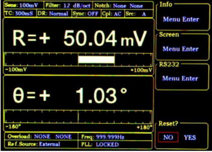
③ Click the button to go to the secondary menu
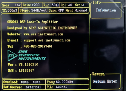
The interface displays information such as the development unit, web address, and version number.
2. Windows Application:
① Find the application ‘SSI OE1022_Console_CN.exe’. If Windows is already connected to the Internet, it will automatically download and search for the driver and install it when you plug in the USB connection between your computer and the lock-in amplifier. If you need to install the driver manually, please refer to the article ‘How to connect the lock-in amplifier via USB in Windows’ for details.
② As shown in the figure, the interface shows the currently connected part:

When you click on the left connection button ‘Connect’, the software will automatically search for serial port resources, if the computer and the lock-in amplifier is successfully connected, the lower window will display the lock-in amplifier version number information, as shown in the figure.

3. Use The Serial Communication to Display The Version Information:
① Each product will be attached to the information disc, which has to talk about the product's remote control serial port / USB2.0 environment and debugging operations. Open the Uart_Assistant folder in the data file, double-click the UartAssist.exe application, the pop-up software interface as shown in the figure:

This serial port debugging software contains communication setting, receive area setting, send area setting, receive area and send area.
② After selecting the serial port and setting the same baud rate as that of the lock-in amplifier, enter ‘*IDN?’ in the send area and end with a carriage return, then click Send. The *IDN? command returns the product model and firmware version.
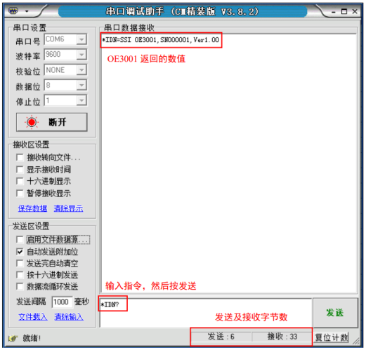
If any data is returned, the version number of the product is displayed in the acceptance area.
Installation And Usage Instructions
Software Installation Steps:
We usually provide the PC software to the user in the form of a disc, which can be run on Windows 7/8/8.1/10 32/64bit systems.
Step 1:
The first step is to install the serial port to USB driver, right click ‘Run as administrator’ Figure 1 red box in the ‘FT232_drive.exe’ file, the software window will pop up as in Figure 2, see the following interface means that the installation of the serial port to USB driver, just wait for the serial port to USB driver, you need to wait for the serial port to USB driver. When you see the following interface, it means the driver of serial port to USB is being installed, you only need to wait for a few minutes.

Fig.1 File
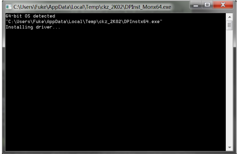
Fig.2 FT232 driver installation screen
Step 2:
If the FT232 driver is successfully installed, a prompt will appear as shown in Figure 3, at this time you only need to follow the prompts to press the ‘Enter’ key to complete the installation of the driver:
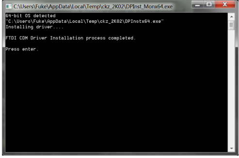
Fig.3 FT232 driver installation completion prompt
In this case, use the USB cable to connect the PC and the lock-in amplifier, and the successful connection will be recognised automatically.
Note:
1. If the PC is already connected to the Internet, when plugging in the USB cable to connect the PC and the lock-in amplifier, it will automatically search for the driver on the Internet and install it.
2. If the PC has already installed the serial port to USB driver, you can skip this step.
3. If the installation is unsuccessful, you can use the inf file to install the driver according to the solution in the ‘readme.txt’ file in the ‘Serial Driver’ directory.
Lock-in amplifier is widely used in temperature detection, photoelectric detection, biological signal detection, geological exploration and so on. The following is its basic application:
Solar Cell Quantum Efficiency Testing
There are two kinds of solar cell quantum efficiency.
External quantum efficiency (EQE): the ratio of the number of charge carriers in a solar cell to the number of photons with a certain energy incident on the surface of the solar cell.
Internal Quantum Efficiency (IQE): the ratio of the number of charge carriers in a solar cell to the number of photons with a certain energy that incident on the surface of the solar cell but not reflected by the solar cel or not penetrate it.
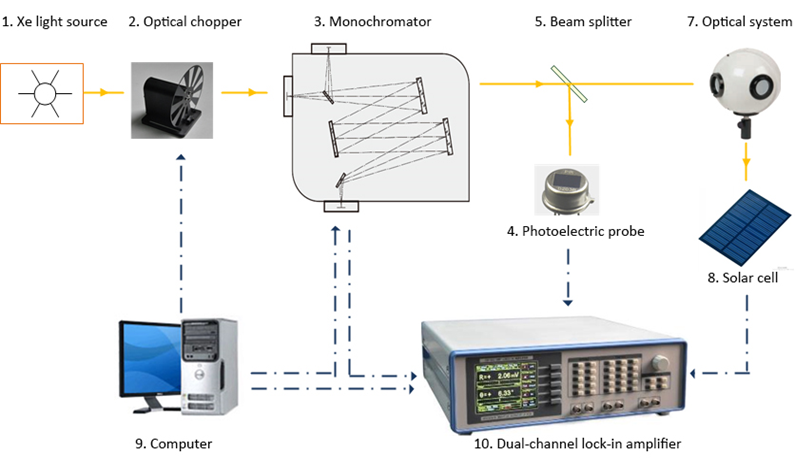
The system of solar cell quantum efficiency detection includes a dual-channel lock-in amplifier, optical chopper, monochromator and other equipment. The probe light emitted from the monochromator is split into two beams. One is converted to photocurrent and input to lock-in amplifier. As a contrast, another light shines on the solar cell and the photocurrent it produces is measured by another channel of the lock-in amplifier. Then the solar cell quantum efficiency can be caculated by the ratio of the two channel results and relevant formula.
Scan Tunneling Spectrum
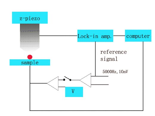
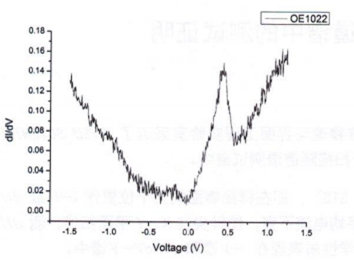
We can obtain scanning tunneling spectroscopy with characteristic peaks by testing I-V/dI/dV at a location on the sample surface. At the characteristic peak voltage, keep the average current constant, so that the tip scan in the X, Y plane and measure the value of dI/dV with the change of X and Y, and then scanning tunneling spectroscopy is got. The electronic and chemical properties of the surface are reflected in the I-V and dI / dV-V spectra.
There are two basic methods for connecting a voltage signal to the lock-in amplifier- the single-ended connection is more convenient while the differential connection eliminates spurious pick-up more effectively.
1. Exterior

Fig.1 Signal input port
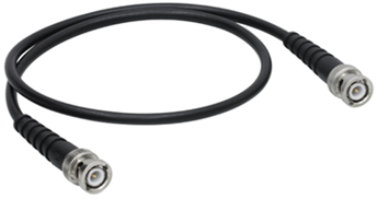
Fig.2 BNC to BNC cable
As shown in Figure 1 and Figure 2, the signal input port is Bayonet Nut Connector. With the matching BNC to BNC cable, you can set up the reliable access from the signal source to the coaxial cable and then to the lock-in amplifier input port.
What's reliability? The most important thing is to minimize any noise that may appear in the measurement system. There may be some sources of external noise (such as engines, signal generators, etc.) in the environment whose influence can be minimized through the carefully designed coaxial cable and BNC connector. Similarly, the difference between the detection probe and the lock-in amplifier can also be solved.
2. Voltage Input
There are two basic methods for connecting a voltage signal to the lock-in amplifier- the single-ended connection is more convenient while the differential connection eliminates spurious pick-up more effectively.
2.1 Mode1: Single-ended Voltage Connecion (A)
The lock-in detects the signal as the voltage between the center and outer conductors of the A input only. The lock-in does not force the shield of the A cable to ground, rather it is internally connected to the lock-in's ground via a resistor. The value of this resistor is selected by the user. Float uses 10 kΩ and Ground uses 10Ω. This avoids ground loop problems between the experiment and the lock-in due to differing ground potentials. The lock-in lets the shield 'quasi-float' in order to sense the experiment ground. However, noise pickup on the shield will appear as noise to the lock-in.
2.2 Differential Voltage Connection (A-B)
The lock-in measures the voltage difference between the center conductors of the A and B inputs. Both of the signal connections are shielded from spurious pick-up. Noise pickup on the shields does not translate into signal noise since the shields are ignored.
When using two cables, it is important that both cables travel the same path between the experiment and the lock-in. Specifically, there should not be a large loop area enclosed by the two cables. Large loop areas are susceptible to magnetic pickup.
3. Current Input
The current input on the OE series lock-in amplifiers uses the A input BNC. For high source impedances, greater than 1 MΩ, and small currents, use the current input. Its relatively low impedance greatly reduces the amplitude and phase errors caused by the cable capacitance-source impedance time constant. The cable capacitance should still be kept small to minimize the high frequency noise gain of the current preamplifier.
4. AC vs DC Coupling
The signal input can be either AC or DC coupled. The AC coupling high pass filter passes signals above 200Hz and attenuates signals at lower frequencies. AC coupling should be used at frequencies above 200Hz whenever possible. At lower frequencies, DC coupling is required.
The traditional lock-in amplifier has many defects due to using analog technology to achieve coherent modulation and greatly limits the phase-sensitive detector accuracy, and also introduces a lot of background noise. Digital lock-in amplifier avoids these and has excellent performance.
Traditional lock-in amplifiers implement PSD through an analog multiplier. But this kind of method that realizes the coherent modulation with the simulation technology has many flaws which will limit the precision of the phase sensitive detector greatly and introduce a lot of background noise. The digital lock-in amplifier does not produce this problem, and has a very high performance.
Embodied as follows:
Excellent Temperature Stability
In addition to the previous stage, the PSD module, low-pass filter and reference circuit of the digital lock-in amplifier have no temperature drift. The deviation of the output is caused mainly by DA conversion and bits accuracy. Meanwhile, the PSD module, low-pass filter and reference circuit of the analog lock-in amplifier all have temperature drift which will introduce serious errors, making a certain error between output and actual results (that is, systematic errors, and it is often with uncertainty).
First-class Noise Suppression
Digital lock-in amplifier will not introduce noise through algorithm calculation and is basically free from interference from the external environment. However, PS and filter build by analog circuits will introduce various kinds of background noise because of limited usage of electronic components. Beside, the ambient noise is also coupled to the analog circuit, and the result of the coherent modulation is incorrect when the magnitude of the background noise is close to the signal or larger than the signal. The dynamic reserve of the phase-sensitive detector realized by analog technology is basically limited to below 60 dB. The dynamic reserve of the PSD realized by digital technology can reach 90dB or more. For example, the dynamic reserve of OE1022 is up to 100dB.
Excellent Harmonic Suppression Performance
As devices evolve, the reference signal of digital lock-in amplifier, such as OE1022 can achieve 24-bit or higher bit-widths. In PSD module, suppression of harmonic components enables distortion of -90db or lower. In addition, due to the usage of digital filters, it will not introduce harmonic distortion caused by op amps.
Low-cost And High-performance Low-pass Digital Filter
the digital filter structure is simple and easy to debug. Since the front and rear filter have no effect to each single-stage filter, the low-pass filter can be made very steep and can be freely selected. The filter of OE1022 is divided into 6,12,18,24dB / oct and time constants extrend from 10us to 3000s. The center frequency of analog filter will change with different devices characteristics and temperature drift, which make a hard debug and introduce some of the error.
High-capacity Digital Storage - for Ultra-low Frequency Measurements
For low-frequency signals, the general filter is powerless or with little effect after filt out the AC component. Then you need to use synchronous filter, which is equivalent to a very good low-pass filter, to average data in a period. It requires a large external circuits to realize a good synchronous analog filter. It's an unwise choice from cost so that its low frequency signal measurement is usually not too low. Meanwhile, digital filter can store a huge amount of data through its large capacity. Now OE1022 can achieve the time constant of 3000s, which is the base of 1mHz frequency measurement accuracy.
The basic function of the lock-in amplifier is to extract the target signal from the noisy environment. In all electronic systems, noise is ubiquitous. According to the cause of the noise, it can be roughly divided into two types: the internal noise of the system (intrinsic noise) and the external environmental noise. From the microscopic point of view, the internal noise is generated due to the randomness of the instantaneous motion of the carrier. This randomness leads to the fact that we can not accurately predict the instantaneous value at any future moment, that is, the system noise is introduced. To the external noise, some unpredictable interference outside the system will cause the system's internal response, causing system error. From a subjective point of view, any signal that is not wanted or that affects the measurement can be considered as noise. Although the noise has the unpredictable characteristics with instantaneous value, but such randomness is not completely chaotic, they have a certain statistical law.
1. Common Noise Source of Electronic System
1.1. Thermal Noise
No matter whether the system is working or not, the thermal noise exists in any electronic system. Even if the system is not powered, the electronic device will exhibit noise characteristics. Thermal noise was first discovered by J.B. Johnson in 1928, so thermal noise is also known as Johnson noise. The voltage of thermal noise can be calculated by the following formula:
Vnoise (rms)=(4kTR△f)1/2
In the above formula, k is the Boltzmann constant with a value of 1.38 × 10⁻²³ J / K. T is the Kelvin temperature. R is the resistance of the resistor in ohms Ω and Δf is the measured bandwidth. As can be seen from the above equation, the power spectral density function of thermal noise has nothing to do with the frequency. When the temperature and the resistance value is constant, the power spectral density function is a straight line, indicating that the thermal noise has the property of white noise.
1.2. Shot Noise
Shot noise usually exists in the PN junction. The micro-mechanism is that the random emission and annihilation of carriers in the PN junction cause the current flowing through the barrier to randomly fluctuate. Shot noise was first discovered by W. Schottky in 1918 in a study of hot cathode tubes and it was theoretically proved a kind of white noise. Shot noise can occur as a noise current in the current measurement and is given by the following formula:
Inoise (rms)=(2qI△f)1/2
In the above formula, q is the electronic element charge and its value is 1.62 × 10⁻¹⁹C. I is the effective value of AC current or average value of DC current of the PN junction. △ f is the measured bandwidth. To system or environment with small bandwith, shot noise generally has a negligible effect and it can be ignored.
1.3. Noise
1 / f noise was first discovered by Johnson in 1925 in tube current. For resistive elements with the same resistance and different materials, they have the same thermal noise. When the two conductor contact is not ideal, their contact resistance will be random fluctuations, which caused the noise, called 1 / f noise. The salient features of the noise is its power spectral density inversely proportional to the operating frequency f. So that, the lower the frequency, the more serious the influence of noise. The power spectral density function is:
Sf(f)=(KId2)/f(V2/Hz)
In the above formula, K is a fixed value which is related to the material type, contact surface, geometry and others. Id is the average DC current flowing through the conductor and the unit is A; f is the operating frequency. The 1 / f noise of carbonaceous resistors is typically 0.1-0.3μVrms. The noiseof metal film resistors or winding resistors is approximately 1 order of magnitude smaller than the carbonaceous resistance.
1.4. Total Noise of The Electronic System
The internal noise of the electronic system described above is independent of each other. If the total internal noise of the electronic system is described statistically, we should square the RMS values of the independent noise sources and then accumulate and carry out the operation. At last we get the total noise.
2. External Noise Source
In addition to the above-mentioned internal noise of the electronic system, various interferences from the external environment may appear during the experiment. Most external noise sources are asynchronous with the system in the time domain. In the frequency domain, these noises are not related to the reference signal frequency and the harmonics of the reference source in the system. These noises may come from lighting Equipment, refrigeration equipment, motors, radios, computer screens and so on. Eliminating the above noise will increase the requirements for dynamic reserve and time constant of the measurement system.
Some external noise sources may have synchronization and correlation with the source signal in the system. When these external noise is introduced into the system, it will cause serious distortion of the target signal, such as fluctuation in the target signal amplitude. This distortion can not be ruled out by frequency-dependent methods, that is, the lock-in amplifier will consider this part of the noise as the source signal, resulting in a measurement error. A typical source of synchronous noise comes from the in-ground current design of the experimental environment and instrumentation. External noise sources can couple into the source signal path in a variety of ways.
2.1. Effect of Capacitive Coupling
Imagine an AC voltage signal close to the measurement environment, which may be coupled to the path where the detector is located by a parasitic capacitance. Although the parasitic capacitance may be very small, the noise generated by coupling may be much larger than the weak signal under test, especially when there is synchronization and correlation between the coupling noise and the source signal in the system.
The lock-in amplifier will see all signals on the target frequency as the source signal. If the AC voltage signal is a high-frequency signal, the coupling noise gain will be more obvious.


